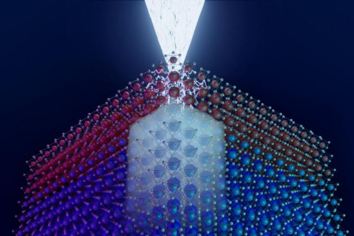


It has long been a dream to invent new materials from the “top down” choosing which atoms go where to engineer properties of interest. A technique created by Pittsburgh Quantum Institute-led researchers may help scientists and engineers “sketch” patterns of electrons into a programmable quantum material–lanthanum aluminate/strontium titanate or “LAO/STO.” Using this approach, they can create quantum devices and with feature sizes comparable to the spacing between electrons, and even “sketch” artificial lattices for electrons to traverse, with extremely high precision, according to a university news story.
To develop this capability, the researchers repurposed an electron beam lithography instrument, which is ordinarily used to create nanostructures by exposing a resist that hardens into a mask, enabling layers of material to be subsequently added or removed. Instead of operating the instrument at its usual value of 20,000 Volts, the researchers dialed it down to only a few hundred volts, where the electrons could not penetrate the surface of their oxide material, and instead–without any resist–catalyze a surface reaction that renders the LAO surface positively charged, and the LAO/STO interface locally conductive.
The electron beam is 10,000 times faster at writing compared with atomic-force microscope-based lithography, without losing spatial resolution or ability to be reprogrammed. In addition, the authors showed that this technique can program the LAO/STO interface when integrated with other 2D layers such as graphene.
The team is led by Jeremy Levy, a Distinguished Professor of Condensed Matter Physics and director of the Pittsburgh Quantum Institute, describe the method in the paper, “Nanoscale control of LaAIO3/SrTiO3 metal-insulator transition using ultra-low-voltage electron-beam lithography.” The paper was published in Applied Physics Letter on Dec. 21.
Dengyu Yang, a graduate student who developed the technique and is lead author on the paper, compared it to “imaging a sketch on a canvas with a pen.”
“In this case, the canvas is LAO/STO and the “pen” is a beam of electrons. This powerful ability allows us to participate with more complex structures and expend the device from one dimension to two dimensions,” she said.
Yang and Levy said the discovery could have implications in the fields of quantum transport and quantum simulation.
“We are very interested in using this technique to programmatically create new families of two-dimensional electronic materials based on arrays of artificial atoms written using this technique. Our group recently published a paper in Science Advances demonstrating the idea of quantum simulation in one-dimensional devices, using the AFM method. This new EBL-based technique will enable us to perform quantum simulation in two dimensions,” said Levy.
In addition to Yang and Levy, Pitt collaborators on the paper include research professor Patrick Irvin and graduate students Shan Hao, Qing Guo, Muqing Yu, Yang Hu, Assistant Professor Jun Chen from the Swanson School of Engineering. Additional affiliations include the Department of Materials Science and Engineering at University of Wisconsin-Madison and Pittsburgh Quantum Institute.